


If you have a DECO version of Astro Fighter, the boards are not totally interchangeable with those from the more common Gremlin version. Below are differences that I've been able to ascertain:
I/O Board:
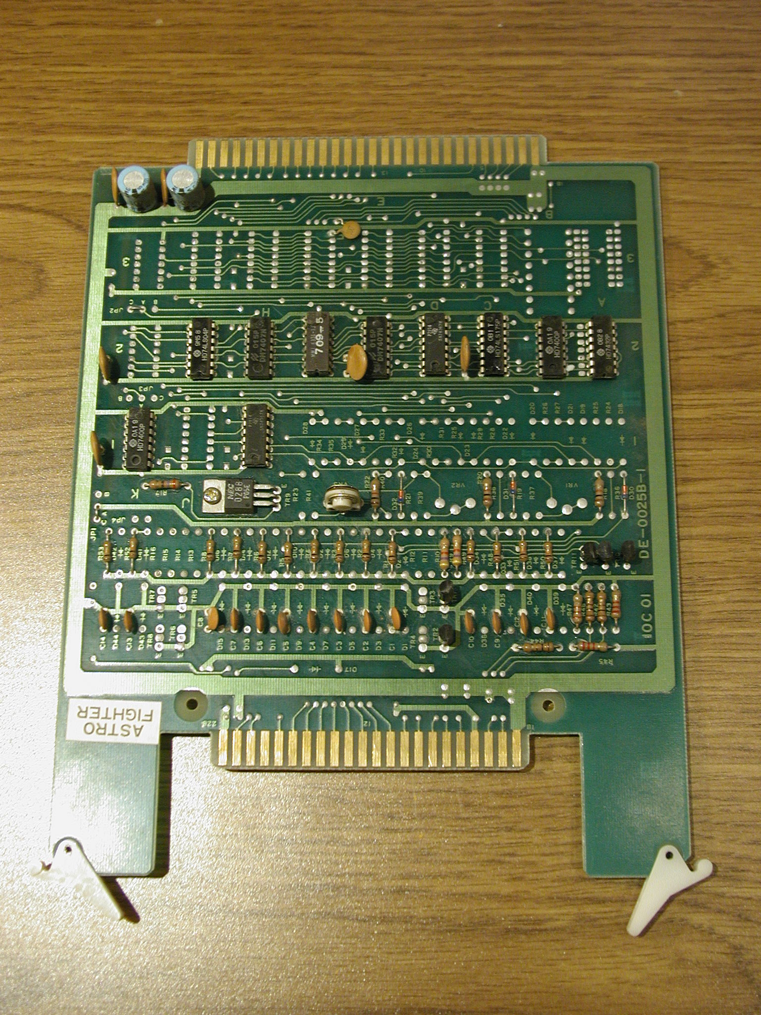
DO NOT PLUG a Sega I/O board into a DECO cabinet - It seems to do bad things to the monitor!!
Sega CPU and ROM/Sound board can be switched as matched pairs into a DECO cabinet with the following issues:
- The screen is upside down
- There is no sound
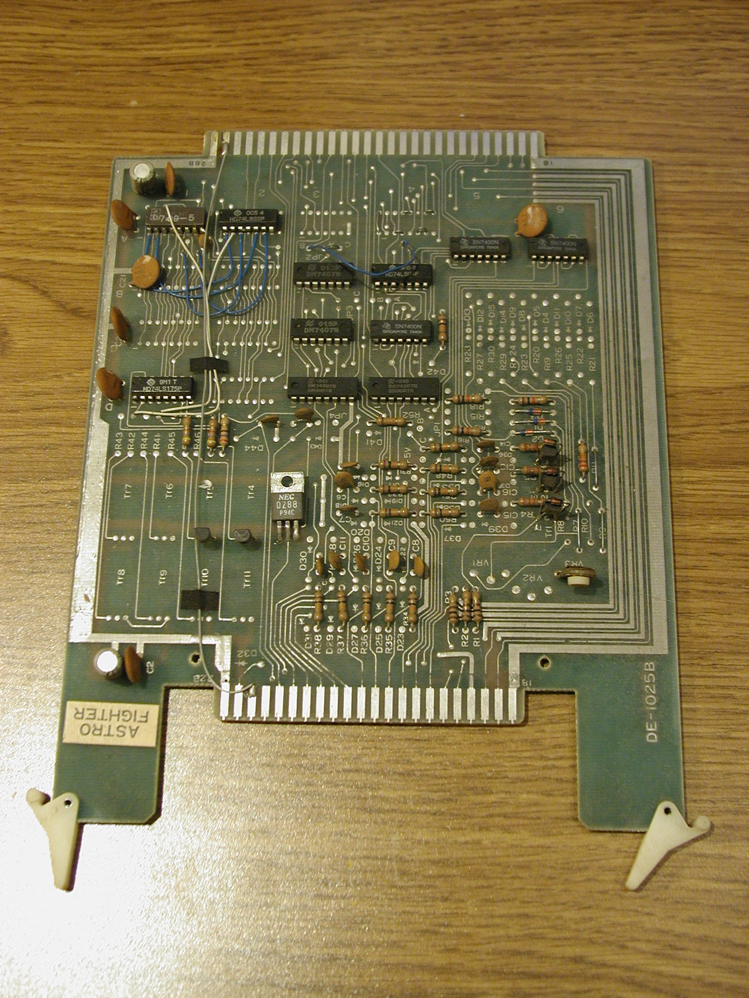
CPU Board:
Sega board has the following changes:
Parts Side:
- Wire patch: 4L pin 8&9 (wire touches both pins) to 5J pin 3
- Leg lifted 5J pin 3
- Wire patch: 4L pin 10 to 5J pin 12
- Trace cut: above #6 at A6
- Trace cut between legs 10&11 of IC A6
- Trace bridged with solder from 6H pin 3 to 6F pin 4
- Trace cut: from 6H pin 4
Solder Side:
- Both boards have a wire patch from Edge Connector 3A to 5B pin 7
- Wire patch: Right side of [Cap 6A] to IC 6A pin 5
- Wire patch: 6A pin 6 to 4A pin 5
- Trace cut: 6B between pins 3 and 4
- Solder bridge 6A pins 3 and 4
- Wire patch: Edge Connector 2A to E4 middle of the CPU chip (which has a trace going to pin 7 of E3)
- Wire patch: Edge Connector 19A to F6 pin 8
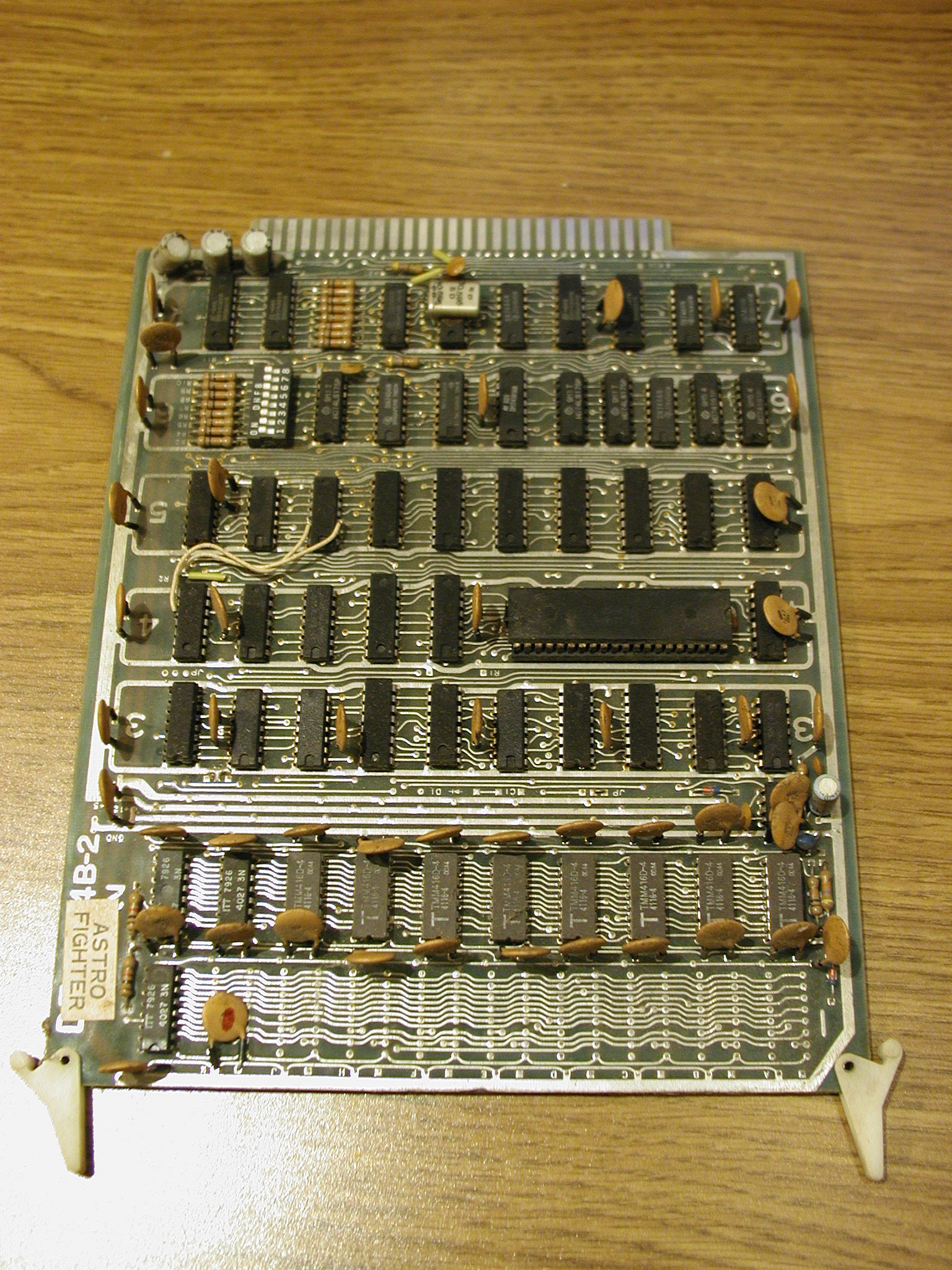
ROM Board:
DECO and Gremlin: DE-1022B-2
Sega board has the following changes:
Solder Side:
- Wire patch from M3 pin 14 to Edge Connector 3A
- Wire patch from M5 pin 2 to Edge Connector 2A
Sound Board:
DECO and Gremlin: DE-0038B-1
Sega board has the following items removed/changed:
Parts Side:
- Removed: VR2 a 10K POT similar to VR1
- Removed: C78 220mfd @ 16V
- Removed: C76 100uf @25V
- Trace cut between pin 1 of IC15 (the Amp) and + of C76
- Removed: C72 220mfd @16V
- Wire patch from pin 1 of VR2 to (-) side of C78
Solder Side:
- Wire patch: CNB (Ribbon Connector) Pin 2 to IC3 pin 1
- Trace cut between CNA (Ribbon Connector) pin 1 and IC 3 pin 1
- Trace cut at CNB pin 1